


![]()
Relevant publications:
A Microtransceiver for UHF Proximity Links Including Mars
Surface-to-Orbit Applications
Kuhn, W., Lay, N. E.,Grigorian, E.; Nobbe, D.; Kuperman,
I.; Jeon, J.; Wong, K.; Tugnawat, Y.; He, X.
Proceedings of the IEEE, Vol. 95, Issue 10, pp. 2019-2044,
Oct 2007
A UHF Proximity Micro-Transceiver for Mars Exploration
Kuhn, W.; Lay, N.; Grigorian, E.
2006 IEEE Aerospace Conference, 4-11 March 2006
Low temperature performance of COTS electronic components for Martian
surface applications
Tugnawat, Y. and Kuhn, W.
IEEE Aerospace Conference, 2006, 4-11 March 2006
A Low-Volume, Low-Mass, Low-Power UHF Proximity Micro-Transceiver for
Mars Exploration
W. Kuhn; N. Lay; and E.Grigorian
12th NASA Symposium on VLSI Design, Oct 4-5,
2005
Low Temperature Performance of COTS Electronic Components for Future
Mars Missions
Y. Tugnawat; and W. Kuhn
12th NASA Symposium on VLSI Design, Oct 4-5,
2005
Low Temperature Performance of Commerical-Off-The-Shelf (COTS) Electronic
Components for Future Mars Missions
YOGESH TUGNAWAT M.S., Kansas State University, 2004
![]()
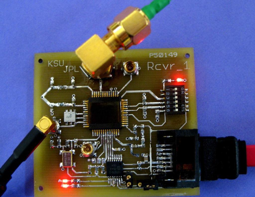
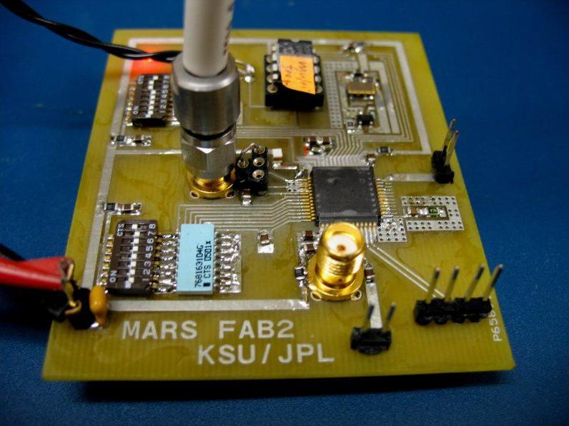
Mars PCB
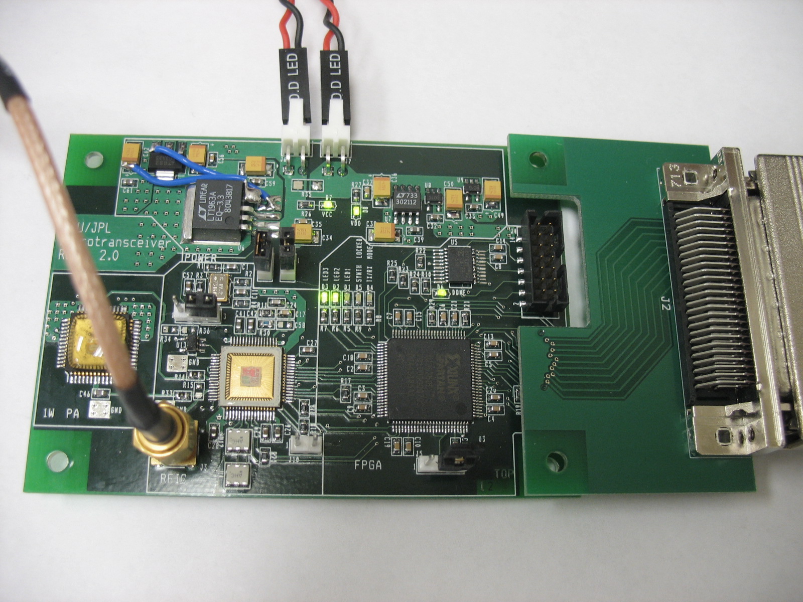
One large project recently completed at KSU involved the development of RF communication ICs for NASA's Mars rover missions. This project is well documented and may be found here. Funded by NASA and JPL through the "Mars Technology Program," the ultimate goal was to develop a low-weight and low-power RF communication circuit for future missions to Mars. At the time, the communication device that was used on the Mars rover weighed 2 kg and consumed up to 70 Watts of power. There was an obvious need for much smaller devices capable of communication, and by the project's end the final product consumed less than 2 Watts of power and could fit in a pocket. This final product is pictured below.
Early PCB Testboards
Over the course of the design process, many different revisions
of the transceiver chip were required as the final product developed,
along with corresponding PCBs. Documentation regarding this
process may be found
here.
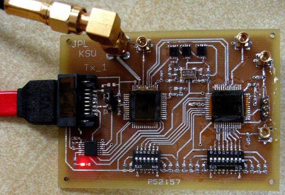
The first PCB developed was a proof-of-concept, and used manufactured
ASICs for both RF communication and digital encoding. This PCB is
photographed below.
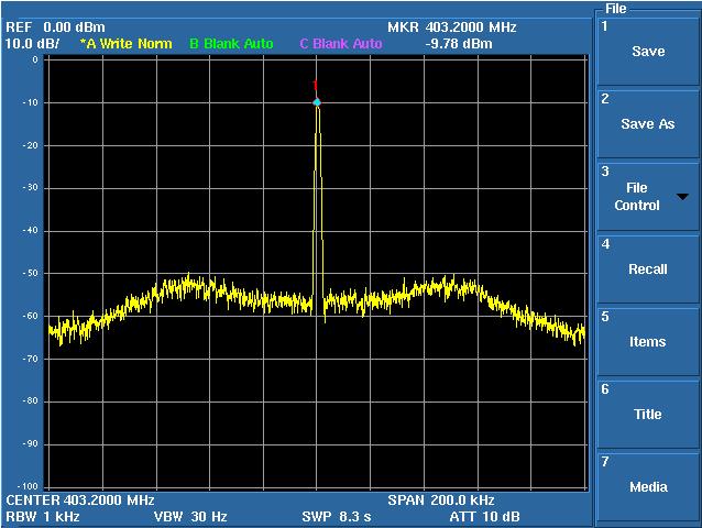
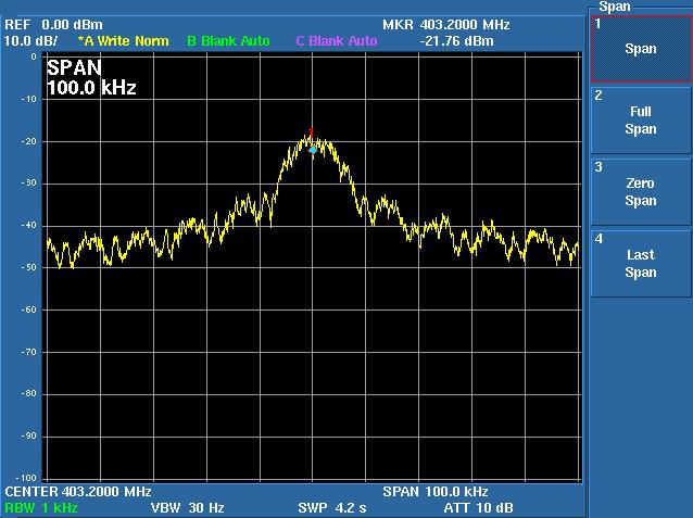
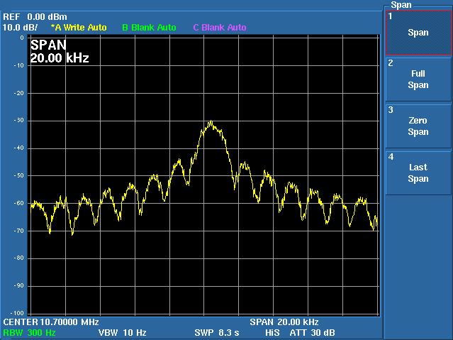
This board was fully tested at using KSU's Microwave design lab's equipment. Pictured below are outputs from a spectrum analyzer, showing the board transmitting a signal at 403.2 MHz, the frequency the Mars transceiver was designed for. The second image is a zoomed-in version of the first.
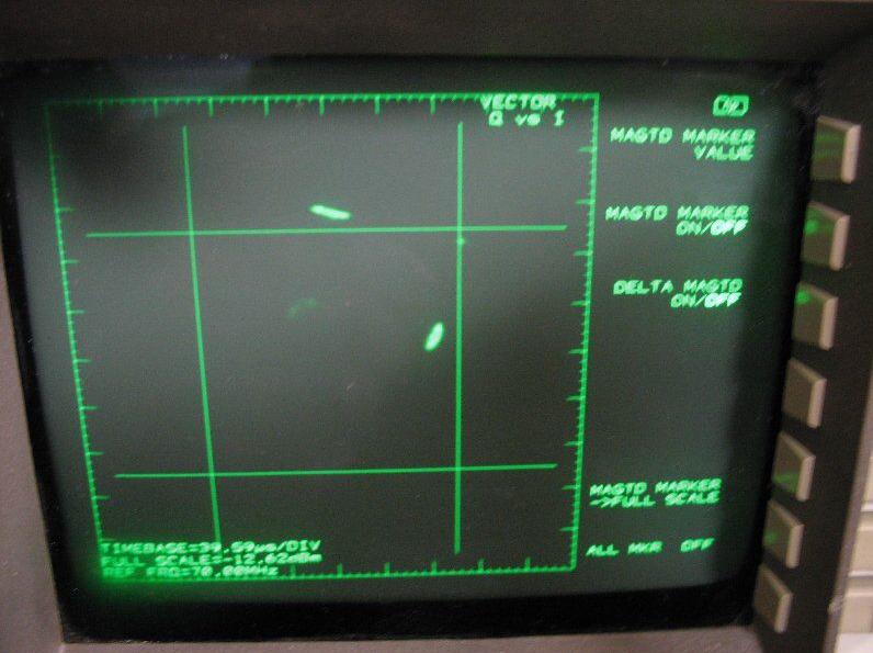
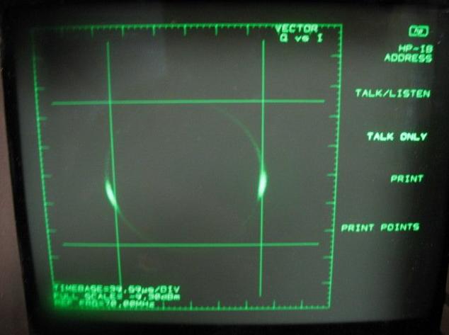
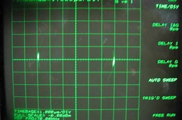
The preferred encoding scheme for this project was BPSK (though RC-BPSK and QPSK are also available). To that end, constellation plots were also taken from the testboard to ensure that the RFIC was modulating information correctly. The two pictures below are of constellation plots taken from a Vector Network Analyzer, used by KSU's Communications Research Lab.
At this point in the design process, It was shown that a device built upon the basic tenants of the above PCB would be suitable for communication applications. The next step was to develop an RFIC receiver unit capable of operation on the Mars surface (which required cryogenic testing). After fabricating and testing a receiver RFIC, designed at KSU, it was implemented on a testboard so that performance measurements could be taken.
Early Receiver-Based Testboard
A picture of the testboard that included this RFIC receiver is shown
here:
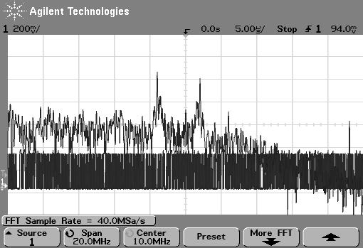
Now outfitted with a custom-made IC and a digital encoder, the spectrum of the output of the board needed verification. Below are images produced from test equipment used to verify that the analog-to-digital signal was correct. The second image is an FFT of the spectrum shown in the first.
Having verified the receive unit, it was desired to design and fabricate an RFIC transmitter, which would later be implemented onto a single chip as part of the Mars Microtransceiver research project.
Early Transmitter-Based Testboard
After developing the RFIC transmitter unit, it was implemented onto a new PCB. This testboard is shown below.
This board was tested to ensure correct operation when using BPSK and RC-BPSK encoding schemes, running at 1 kbps. The output of the testboard, when emitting a BPSK signal, is pictured here.
The output of the testboard, when emitting an RC-BPSK signal, is pictured here.
Two more intermediary PCBs were developed and tested, until the final product was completed. This final board is discussed below.
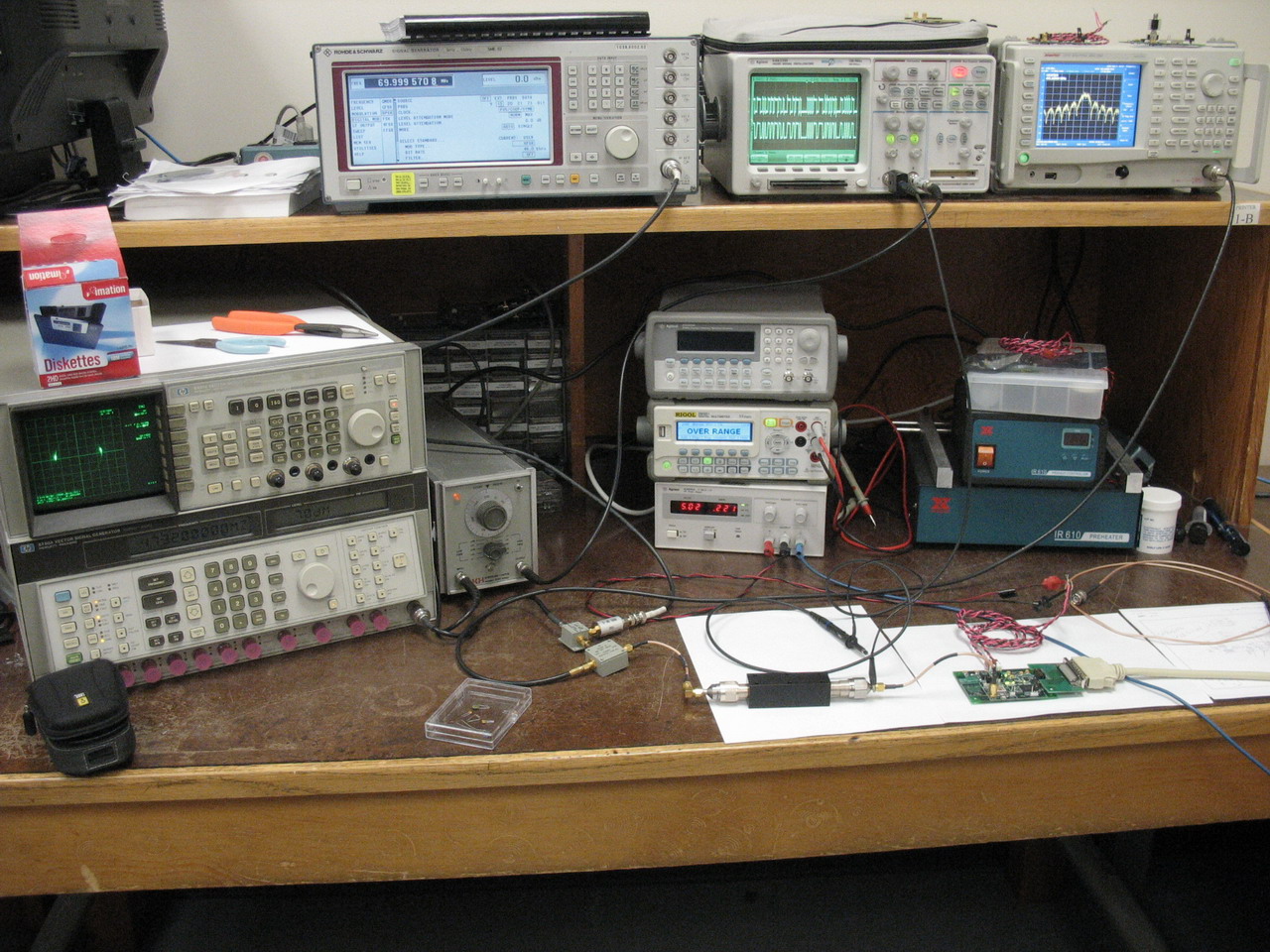
Final Evaluation Board Testing
The final evaluation board is seen below:
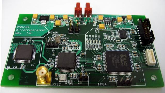
This board was intended for NASA Mission planners. The board, developed entirely by KSU and JPL, is under consideration for future "scout" missions on the Martian surface, where temperatures can reach as low as -120 °C. Below is an image of the testing environment. Within the picture there is the output of the BPSK ADC on a spectrum analyzer, a constellation plot of the output on a vector network analyzer, and transmitted/received data-streams on an oscilloscope.
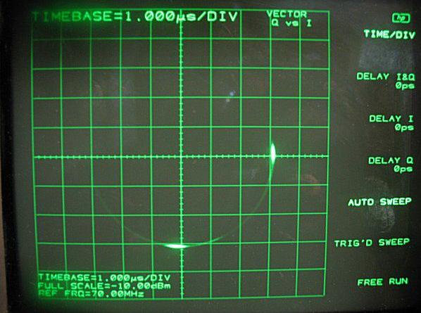
Finally, the video below shows how the data on the vector network analyzer is affected by phase noise. The two points that are revolving around in a circle are BPSK outputs, and move because the unmatched phases between all the devices in the test setup.