|
Scope
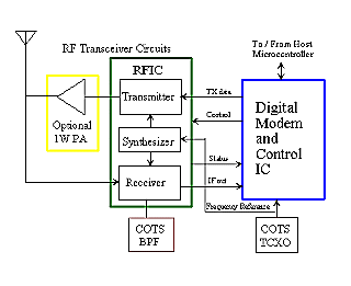
This page provides an overview of the RFIC design work with emphasis on the top-level architecture and interfaces. Detailed documentation including schematics, design documents, and layout files are provided on the project's secure web site. Scout mission planners requiring access to this information should contact project personnel.
RFIC Architecture
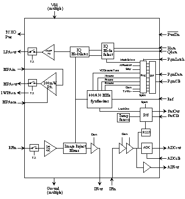 The detailed architecture of the RFIC die
is shown here. For reliability enhancement
and development risk-reduction, it employs relatively traditional
direct-conversion transmitter and superheterodyne receiver architectures
operated in a half-duplex mode. Both
share a common UHF synthesizer which generates the necessary quadrature
sinusoids needed for IQ modulation and for image-reject mixing. The synthesizer operating frequency, as well
as most control functions of the IC, are programmed through a 3-wire serial buss
with CMOS logic levels. The detailed architecture of the RFIC die
is shown here. For reliability enhancement
and development risk-reduction, it employs relatively traditional
direct-conversion transmitter and superheterodyne receiver architectures
operated in a half-duplex mode. Both
share a common UHF synthesizer which generates the necessary quadrature
sinusoids needed for IQ modulation and for image-reject mixing. The synthesizer operating frequency, as well
as most control functions of the IC, are programmed through a 3-wire serial buss
with CMOS logic levels.
A single synthesizer is feasible due to the
half-duplex operating mode. This
conserves power and die area and allows the elimination of bulky duplex
filters and of their noise-figure penalties. In addition, it permits the
co-location of power amplifier circuits on the same die as the sensitive
receive circuits. During transmit, the
synthesizer is programmed to the desired output frequency (e.g. 404.4 MHz) by
the digital baseband/control IC. During
receive, the synthesizer is programmed to the receive frequency (e.g. 435.6
MHz) plus the IF (nominally 10.7 MHz).
This high-side injection strategy is used to provide better tracking of
the TCXO and IF filter drift with temperature as described in the Cryogenic Electronics page of this site.
 Within an application circuit, the system’s
antenna is connected simultaneously to the RFIC’s LNA input and one of the PA
outputs as shown here. During transmit mode, a
reflective switch at the input to the LNA steers the transmit signal to the
antenna and protects the LNA from the large voltages associated with 100 mW to
1 W operation (when using the optional external 1 W PA IC). See the Transceiver Testing page for measured S11 plots of the LNA in transmit and receive conditions. During receive, the transmitter outputs
become reflective terminations so that the majority of the receive signal power
is routed to the LNA, minimizing noise figure.
These reflective terminations are represented by the open-circuit
switches shown in the block diagram above, although the actual implementations employ
parallel-resonant tanks which are combined with impedance-matching
circuits. Details of the resonant
switch design can be found in this paper. Within an application circuit, the system’s
antenna is connected simultaneously to the RFIC’s LNA input and one of the PA
outputs as shown here. During transmit mode, a
reflective switch at the input to the LNA steers the transmit signal to the
antenna and protects the LNA from the large voltages associated with 100 mW to
1 W operation (when using the optional external 1 W PA IC). See the Transceiver Testing page for measured S11 plots of the LNA in transmit and receive conditions. During receive, the transmitter outputs
become reflective terminations so that the majority of the receive signal power
is routed to the LNA, minimizing noise figure.
These reflective terminations are represented by the open-circuit
switches shown in the block diagram above, although the actual implementations employ
parallel-resonant tanks which are combined with impedance-matching
circuits. Details of the resonant
switch design can be found in this paper.
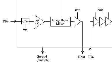 In receive mode, the switch shown in-line with
the RFin signal is effectively closed and the signal encounters approximately
16 dB of power gain in the tuned-RF LNA followed by approximately 20 dB of gain
within the image-reject (IR) mixer. IR
mixing is employed to minimize noise figure only. Actual image signal rejection is not a critical performance
parameter within the Mars environment.
Similarly, since the interference environment at Mars is more benign
than that in terrestrial radio systems (e.g. cell phones), low input compression
can be traded for low power operation.
Further, to optimize noise figure performance, only limited filtering
provided by the matching circuits is used in front of the LNA. These issues should be carefully considered
by the system designer to guarantee electromagnetic compatibility with other electronics
onboard the scout craft. A preliminary EMC mask is given by the measured spurious response plot here. In receive mode, the switch shown in-line with
the RFin signal is effectively closed and the signal encounters approximately
16 dB of power gain in the tuned-RF LNA followed by approximately 20 dB of gain
within the image-reject (IR) mixer. IR
mixing is employed to minimize noise figure only. Actual image signal rejection is not a critical performance
parameter within the Mars environment.
Similarly, since the interference environment at Mars is more benign
than that in terrestrial radio systems (e.g. cell phones), low input compression
can be traded for low power operation.
Further, to optimize noise figure performance, only limited filtering
provided by the matching circuits is used in front of the LNA. These issues should be carefully considered
by the system designer to guarantee electromagnetic compatibility with other electronics
onboard the scout craft. A preliminary EMC mask is given by the measured spurious response plot here.
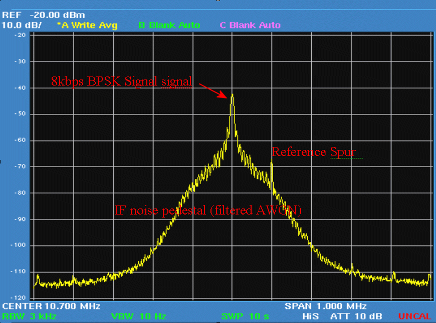
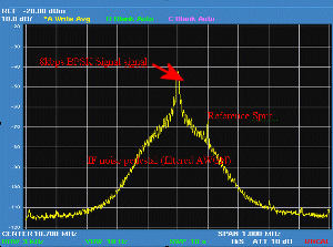 Following downconversion, the received
signal is amplified at a 10.7 MHz intermediate frequency. The IF signal is routed off-chip to a Commmercial Off-the-shelf (COTs) ceramic IF
filter which restricts the bandwidth to approximately 300 kHz. This bandwidth provides the spectrum
narrowing required to prevent saturation of later stages of the IF amplifiers
by broadband downconverted noise. In
addition, it is needed to provide adequate prefiltering for 1-bit
analog-to-digital conversion and subsequent demodulation functions in the
digital modem/control IC. This figure shows the spectrum at the output of the IF filter with an unmodulated carrier on-channel. The characteristic noise-pedistal is seen, together with an 8 kbps BPSK signal within the passband center. Following downconversion, the received
signal is amplified at a 10.7 MHz intermediate frequency. The IF signal is routed off-chip to a Commmercial Off-the-shelf (COTs) ceramic IF
filter which restricts the bandwidth to approximately 300 kHz. This bandwidth provides the spectrum
narrowing required to prevent saturation of later stages of the IF amplifiers
by broadband downconverted noise. In
addition, it is needed to provide adequate prefiltering for 1-bit
analog-to-digital conversion and subsequent demodulation functions in the
digital modem/control IC. This figure shows the spectrum at the output of the IF filter with an unmodulated carrier on-channel. The characteristic noise-pedistal is seen, together with an 8 kbps BPSK signal within the passband center.
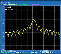 The 1-bit ADC is clocked by an off-chip
signal provided to it from the TCXO or the digital modem/control IC. The transceiver system clock frequency is specified as
19.200 MHz to prevent harmonics of the clock from interfering with receive
signal frequencies and to allow for integer division to data clocks which
conform to Proximity-1 recommended rates up to 256 kbps (division by 75). The clock frequency used for the ADC sampling will be generated within the companion digital IC to optimize its DSP processing. The spectrum shown here is that of the 1-bit ADC output sampled directly at 19.2 MHz (See the Transceiver Testing page for more detail). Note the good dynamic range due to the oversampling of the IF passband width (19.2/0.3). For applications which provide their own ADC
functions, an un-digitized IF output is also provided. The 1-bit ADC is clocked by an off-chip
signal provided to it from the TCXO or the digital modem/control IC. The transceiver system clock frequency is specified as
19.200 MHz to prevent harmonics of the clock from interfering with receive
signal frequencies and to allow for integer division to data clocks which
conform to Proximity-1 recommended rates up to 256 kbps (division by 75). The clock frequency used for the ADC sampling will be generated within the companion digital IC to optimize its DSP processing. The spectrum shown here is that of the 1-bit ADC output sampled directly at 19.2 MHz (See the Transceiver Testing page for more detail). Note the good dynamic range due to the oversampling of the IF passband width (19.2/0.3). For applications which provide their own ADC
functions, an un-digitized IF output is also provided.
Finally, the level of the IF signal entering
either the on-chip or off-chip ADC circuits can be controlled through gain
control bits shifted into the RFIC together with the synthesizer
frequency-control bits. While not strictly needed for operation within a Mars scout to orbiter link, the gain-control may be be helpful in other applications. Twelve bits are
used to provide approximately 72 dB of gain adjustment in approximately 6 dB
steps. The external controller IC can
monitor the level out of the IF chain through the receive signal-strength
indicator (RSSI) circuit periodically to update the gains and form a digital
AGC loop. The RSSI circuit provides 2
bits of resolution as a digital code shifted out of the RFIC using the StatClk
signal. Additional bits shifted out
with the RSSI code include an indication of approximate die temperature and bits
determining if the synthesizer is locked.
Transmit-mode Operation
The transmitter portion of the RFIC implements direct modulation of the synthesizer I/Q outputs using mixers and a summer to produce BPSK, RC-BPSK, or QPSK. This is followed by one or more stages of power amplification. For applications requiring only 10 mW of transmit power, the Medium Power Amplifier (MPA) circuits are disabled and only the LPA is used. For 100 mW applications, the PC board should be configured to route the 10 mW LPA output
to the MPA input. 1 Watt operation employs both the LPA and
MPA together with the optional 1W PA IC.
Transmit mode is entered by programming
the synthesizer for the desired frequency and then bringing the Tx/Rx- control bit high. This signal enables one or both PA circuits
depending on the state of the MPA enable bit and shuts down unneeded receive circuits to
save power. The signal also controls
internal power sequencing circuitry to provide needed spurious emission
reduction and protection of the LNA.
Power Control
The transceiver contains internal power
management circuits to provide for sleep-mode power conservation as well as
near-complete power-down of both itself and the TCXO. Nominal power consumption on receive is 50 mW. This can be reduced to less than 0.5 mW
using a wake/sleep duty cycle of 1 %, and to proportionally lower consumption
with lower duty cycles.
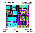
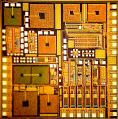
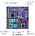
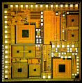
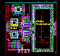
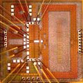
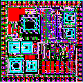
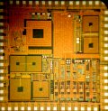
RFIC Layouts
The RFIC circuits were developed through a series of prototype fabrications. Fab 1 contained all the major receiver blocks. Fab 2 contains the first prototype of the LPA and MPA circuits together with an improved synthesizer implementing dual-modulus prescaling and fractional N delta-sigma modulation, plus a revised LNA design with increased gain. Fab 3 contains the prototype 1 Watt PA chip. Fab4 is the final TRL5 version of the full RFIC microtransceiver. It was built by merging designs from Fab1 and Fab2, and improving them where warranted. Each chip is shown below, both in layout view and die photo view forms.
Back to Microtransceiver main page...


|


